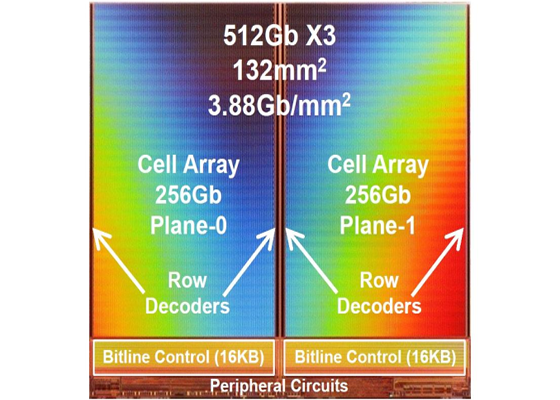
Western Digital’s presentation at the ISSCC reveals that the 512 Gb 3D TLC NAND IC is a dual-plane design with a 132 mm2 die size. From density standpoint, Western Digital’s 512 Gb 3D TLC NAND IC is a little bit behind Samsung’s 64-layer 512 Gb 3D TLC flash chip (which has a die size of 128.5 mm2, according to the company’s presentation at the same conference) that is also a dual-plane IC.
As reported, the current etching tools cannot “drill holes” in a structure that contains ~60 or ~70 wordline layers simply because it is too thick. Therefore to keep using the current tools, makers need to either make the structure thinner or use two separate structures interconnected using the so-called string stacking technology.
To make its 64-layer 3D NAND ICs, Samsung decided to make the structure of its 3D flash memory ICs thinner by making wordline layers (as well as the dielectrics between them) thinner. The move naturally increases the electrical resistance of the wordlines and degrades their retention, which required Samsung to introduce a set of technologies that mitigate the effects of thinner wordlines and dielectrics.